Photonic crystals (Photonic Crystal) was founded in 1987 by S. John and E. YablonovitchProposed independently, it is an artificial microstructure formed by the periodic arrangement of media with different refractive indices. Photonic crystals are photonic bandgap materials, and from the perspective of material structure, photonic crystals are a class of artificially designed and manufactured crystals with periodic dielectric structures at the optical scale. Similar to the modulation of the electron wave function by a semiconductor lattice, photonic bandgap materials are capable of modulating electromagnetic wave — with corresponding wavelengthsWhen electromagnetic waves propagate in photonic bandgap materials, they are modulated due to the presence of Bragg scattering, and the electromagnetic wave energy forms band-structured photonic crystals. There is a band gap between the bands, i.e., the photon band gap. Photons with energy in the photon band gap cannot enter the crystal. Photonic crystals and semiconductors have many similarities in basic models and research ideas, and in principle, people can design and manufacture photonic crystals and their devices to control the motion of photons. The advent of photonic crystals, also known as photon bandgap materials, made possible the dream of manipulating and controlling photons.
1. Huge single-layer polystyrene microsphere array
This product self-assembles polystyrene microspheres into a large-area array structure, and the structure can be used as a template to prepare an antiprotein metal array structure.

Fig.1 Template of polystyrene microspheres with a large area
Scanning electron microscopy (SEM) showed that the Huge polystyrene microspheres exhibited a hexagonal distribution form, and after being bombarded with oxygen plasma gas, the time of the bombardment could be adjusted to form an array structure of polystyrene microspheres with adjustable spacing, as shown in Figure 2. Using this structure as a template, metal nanoarray structures with different spacing and different forms can be prepared, which have a wide range of applications in biological detection and optoelectronic devices.
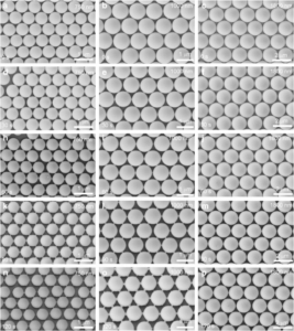
Fig.2 Structure of a single-layer Huge polystyrene microsphere array with adjustable spacing
2. Huge binary metal nanostructure
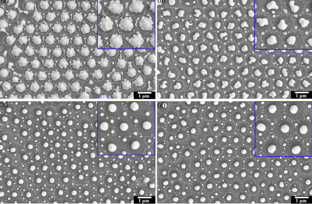
This product is based on the polystyrene microsphere array structure ion sputtering metal film, using the method of high temperature annealing to remove the polystyrene microspheres, on the surface of the substrate can form a binary metal nanostructure, this product takes gold as an example to form a binary gold nanoarray structure.
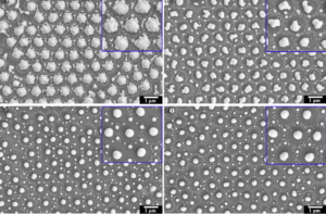
Fig.3 Binary gold nanoarray structure
After sputtering different metal films on the surface of the polystyrene template, the binary metal nanoarray structure of titanium dioxide composite gold nanoparticles was also prepared by high-temperature annealing.
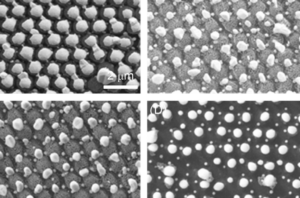
Fig.4 Binary metal nanoarray structure composed of titanium dioxide and gold nanoparticles
3. “Double-faced God” polystyrene microsphere array structure
The single polystyrene microsphere array prepared by the mixed solution interface self-assembly method will form a “double-faced” polystyrene microsphere array structure due to the obvious change of the distribution mode of the binary structure formed by different concentrations.
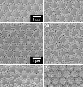
Figure 5: Binary Huge polystyrene microsphere array structure

